Midpoint Status Memo
Overview
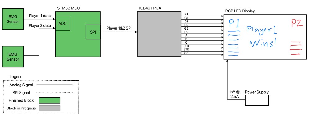
At the midpoint, we are ready to demo our breadboarded EMG sensor and our MCU code, including both the ADC and the SPI peripherals.
Sensor
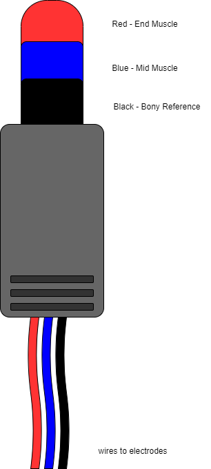

We took inspiration from, but did not fully use, this schematic from a commercial MYG sensor that was out of our budget. This was good for the budget but bad for our time management as we ran into several issues.
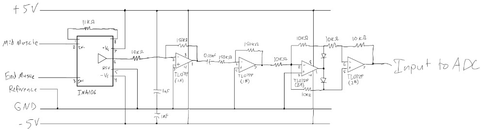
First, when we substitued a different instrumentation amp (the AD623) because we did not have the original schmatic part in the stockroom, we saw a large DC offset. This came from the large resistor we had between reference and ground, which was incorrect and made reference float slightly. We fixed it by connecting it directly to ground. Also, the decoupling capacitor that was meant to remove the DC offset removed the whole signal, so we removed the capacitor. We kept the high pass filter because it was already built into the circuit, and the full wave rectifier because we need it to protect the pins of the MCU. We discarded the rest of the circuit after the rectification because we needed to prioritze the rest of the digital design, not the analog sensor circuits. In total, we kept the instrumentation amplifier stage (with AD623), the inverting amplifier stage, and the full wave rectification stage.
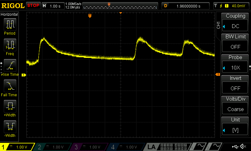
The physical connection to the ADC could be improved for robustness for demo day, but the signal is readable. The signal from a flexed bicep (Ellie’s bicep, to be specific) is in the neighborhood of 1 volt net change. This signal could be increased by having slightly larger gains in the amplifiers, but it will be easily read by the ADC.
MCU
Design
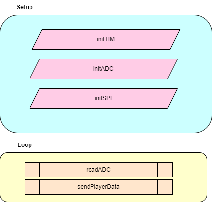
The ADC was our new peripheral for the project, and its device driver is complete and functional. After initializing, ADC1 reads in channels 10 and 11 from pins PA5 and PA6. These will be players 1 and 2 respectively. Each time that the data register is read, the 16 bit data register is stored in a volatile uint_16t. The 16 bits are converted into two characters (8 bits) each, which are stored in an array via a pointer.
The other peripheral in use is the SPI peripheral. A pointer to the char array that the ADC populates is passed into a modified version of the lab 7 SPI code. It sends the 4 chars to the FPGA in the order MSB1, LSB1, MSB2, LSB2.
Testing
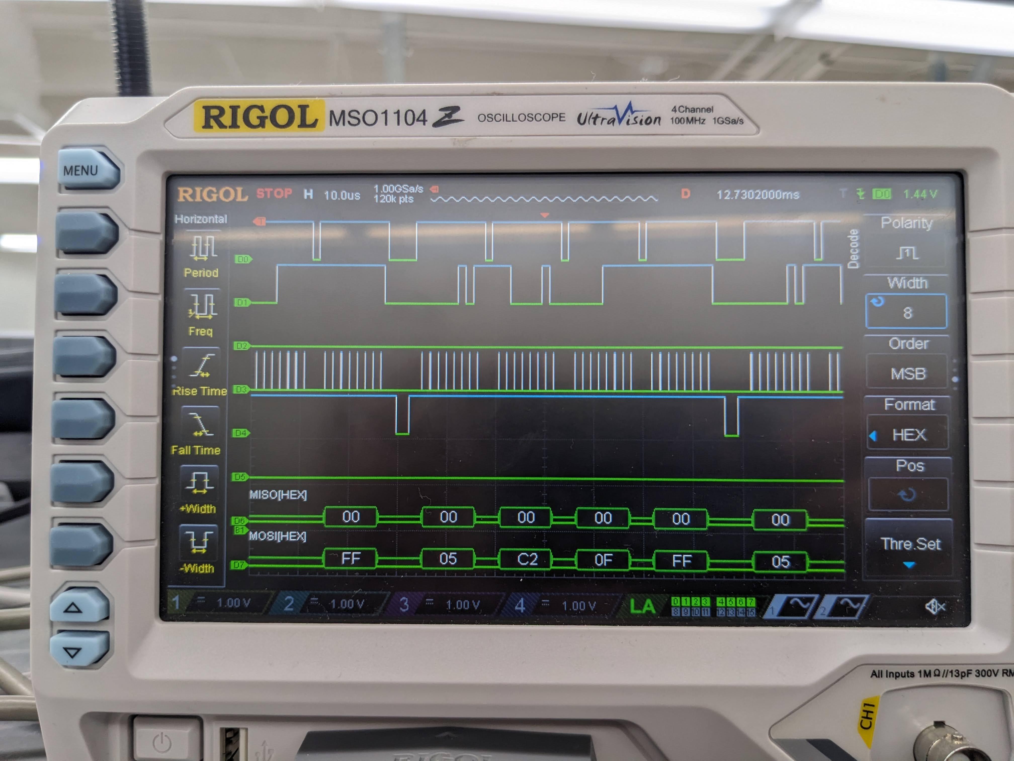
D0 - CS, D1 - MOSI, D2 - MISO, D3 - SCK, D4 - LOAD
As seen in Figure 7, the ADC reads in the values and then the SPI peripheral sends them out. In addition to the regular SPI signals, there is also a load signal that we will use later to tell the FPGA when to shift in new data.
FPGA
Design
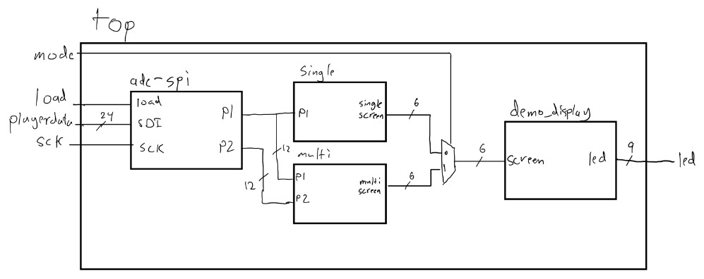
We have designed and started implementation of the FPGA, but it is not yet functional. The design for our first demo_top module is shown in Figure 8. The module that shifts in the SPI data was modified from aes_spi from Lab 7. However, we don’t need to send anything back to the MCU, so SDO will shift out nonsense. Because we intended to only use 12 bits of the received data because our resolution is only 12 bits, all our ports were sized for 12 bits, not 16. This is easily corrected in the top module. The single module has an FSM to determine which screen to show based on who is currently winning and who has been winning most recently. The current setup uses a demo_display module takes that screen and converts it into a simple led bar to show a coarse resolution. This is a temporary setup that will be replaced soon with the full LED matrix module.
Appendix
All our MCU and FPGA code for this project can be found on our Github repo.