Design
Overview
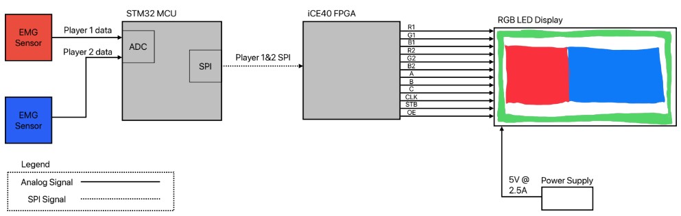
Figure 1 shows the overall system block diagram. The system begins with two amplified signals from the muscle sensors, which is input into the MCU as two analog signals. The MCU then converts the signals into a concatenated 32-bit digital signals and sends the data across SPI to the FPGA. The FPGA reads the SPI signal and contains modules to determine both players’ data and displays them on the LED display through a FSM module that converts a desired screen display into the correct output pins for interfacing with the display matrix. The display matrix interprets the output signals sequentially at a frequency of 1.5MHz to display the screen.
Sensor
An EMG sensor detects electrical activity in muscles via a conductive pad on the skin. Electrical signals on the skin are typically between 50μV to 30mV, depending on the quality of the electrode pads and the individual. An EMG sensor amplifies this signal with a gain between ~33x to 100000x and outputs an analog signal.
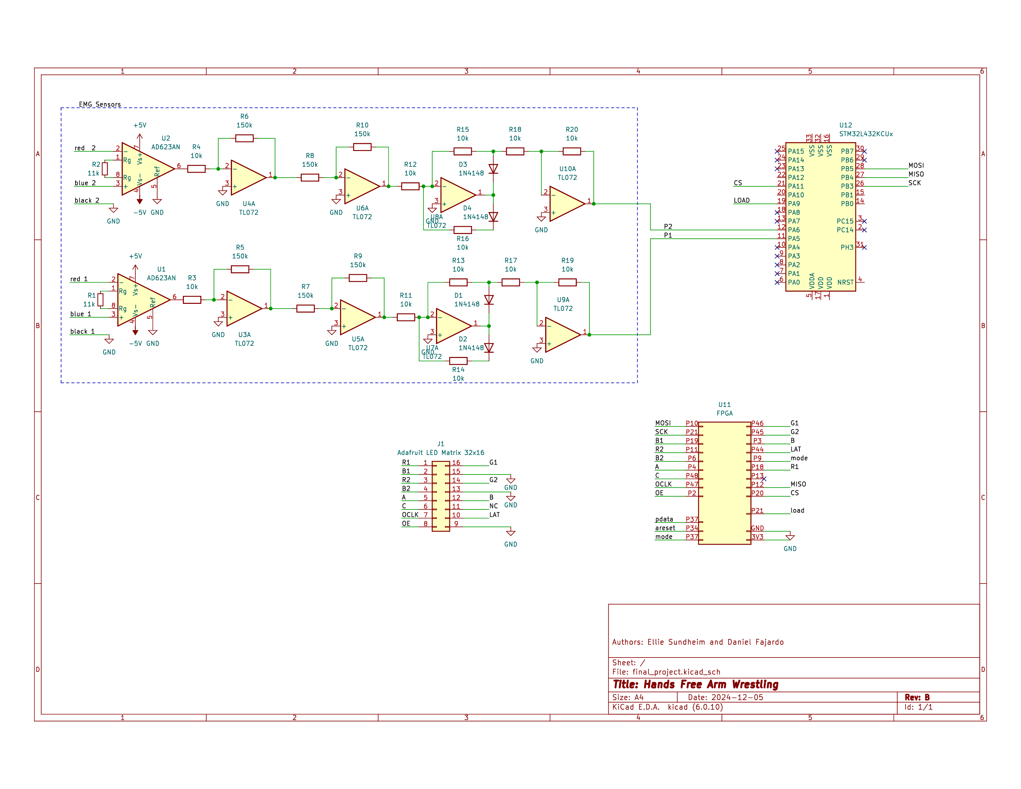
We took inspiration from, but did not fully use, a commercial MYG sensor that was out of our budget. We substituted a different instrumentation amp (AD623) because we did not have the original schematic part in the stockroom. We also removed the decoupling capacitor that was meant to remove the DC offset becasue it removed the whole signal. We kept the high pass filter because it was already built into the circuit, and the full wave rectifier because we need it to protect the pins of the MCU. We discarded the rest of the circuit after the rectification.
MCU
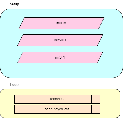
The Analog-to-Digital Converter (ADC) was our new peripheral for the project. After initializing, ADC1 reads in channels 10 and 11 from pins PA5 and PA6, which are players 1 and 2 respectively. Each time that the data register is read, the 16 bit data register is stored in a volatile uint_16t. Because resolution is set to 12 bits (the max), the 16 bit data register has 4 extra zeros at the top. It is easy to get rid of them inside the FPGA, and 16 bits divides nicely into 2 characters of 8 bits each, which is the size of a SPI transaction. The characters are stored in an array via a pointer.
The other peripheral in use is the SPI peripheral. A pointer to the char array that the ADC populates is passed into a modified version of the lab 7 SPI code. It sends the 4 chars to the FPGA in the order MSB1, LSB1, MSB2, LSB2.
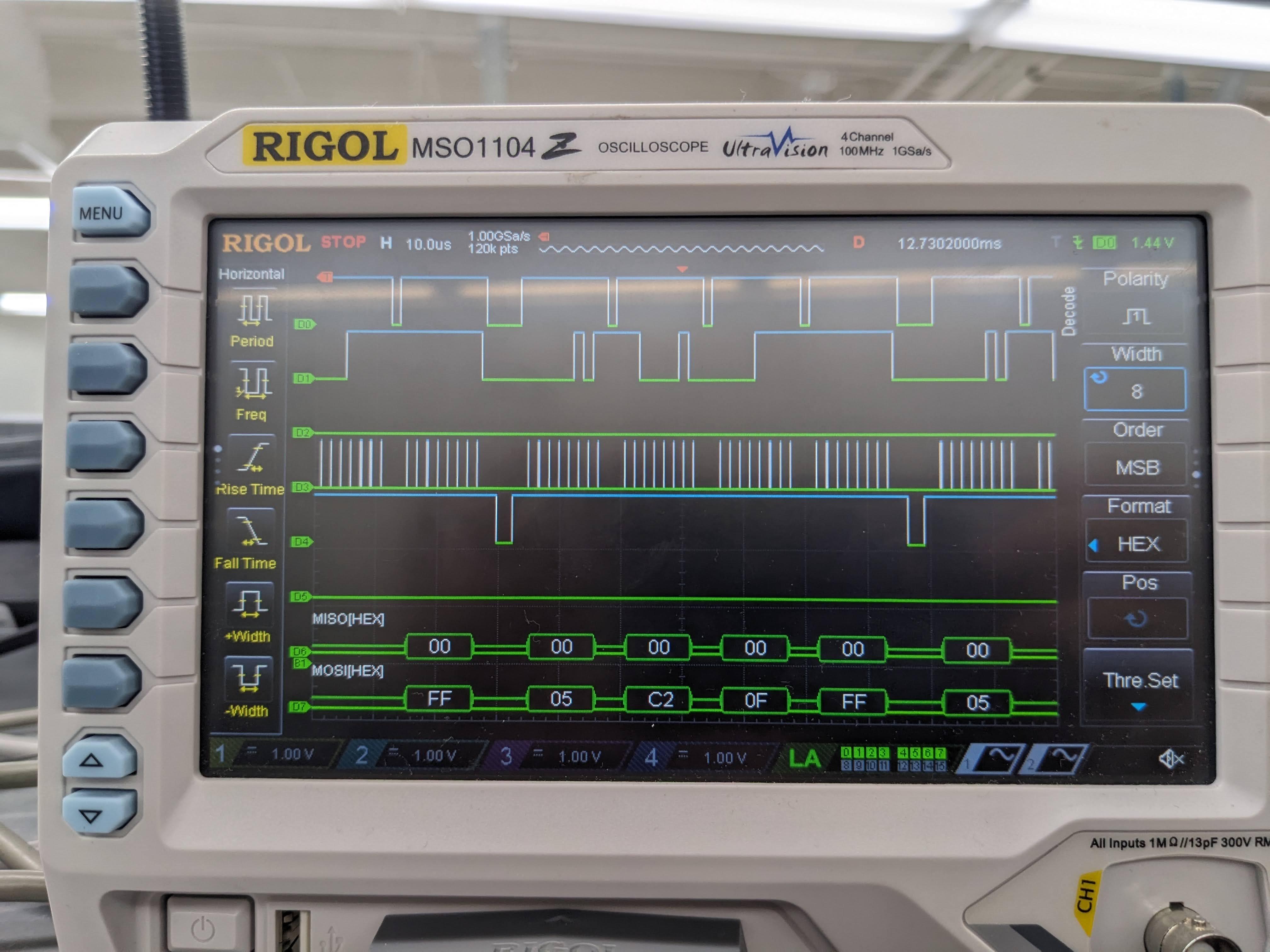
D0 - CS, D1 - MOSI, D2 - MISO, D3 - SCK, D4 - LOAD
As seen in Figure 4, the ADC reads in the values and then the SPI peripheral sends them out. In addition to the regular SPI signals, there is also a load signal that we use to tell the FPGA when to shift in new data.
FPGA
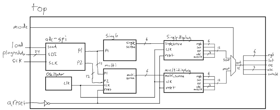
The design for our FPGA is contained in our top module, which is shown in Figure 5. The FPGA design contains a SPI recieve module, two modules for selecting the screen (in single player or multiplayer mode), two modules which interface the selected screen into output pins for the LED matrix, and a multiplex which selects the set of output pins based on the player mode. The module that shifts in the SPI data was modified from aes_spi from Lab 7. However, we don’t need to send anything back to the MCU, so SDO will shift out nonsense. Because we intended to only use 12 bits of the received data because our resolution is only 12 bits, all our ports were sized for 12 bits, not 16. This is easily corrected in the top module.
Once the digital signal is recieved from the SPI module, the single and multiplayer processes are very similar. The single module is an asyncrhonous module, which outputs a 6-bit value for the screen state depending on the input of 1 player’s digital signal magnitude. The multi module is a synchronous module, which also outputs a screen value, but is determined by which players’ digital signal magnitude is greater. The multi module also has some preset screen matrices for winning screens and a start sequence, saved as .txt files.
In the singleplayer pipeline, the 6-bit screen state value is fed to the singledisplay module, alongside the same system clock and reset. Inside this synchronous module, the screen state corresponds directly to the magnitude of the signal and so that value is assigned to a new variable called barrier. This barrier variable denotes which pixels should be lit up, with pixels to the left of it being red and pixels the right being off, to emulate the bar filling effect when flexing harder. The module also writes the entire border as green and contains a
a row above and below the red bar to be off to create a more stark contrast.
In the multiplayer pipeline, the multipdisplay module functions very similar. It is also synchronous, and takes in a new set of 21 screen states. Again, the barrier method is used for the first 15 screen states, with pixels left of the barrier being red, and pixels to the right being blue. Similar border and buffer rows are written again as well. The multidisplay module has an additional six screen states for the start sequence and player winning screens. These screens are created using text files with a 16x32 matrix of 1s and 0s to mark whether the pixel is on or off. These text files are read sequentially and the appropriately mapped pixel is on for 1 and off for 0. Because the display is capable of rgb, this method restricts the leds to just one color.
To correctly interface with the LED display, the singledisplay and multidisplay modules we need to output two sets of 3-bit rgb values, a 3-bit abc value to select the row in the matrix, a latch, an output enable, and a clk. The matrix works by sequentially turning on two pixels at a time on each clock pulse. The two rows are selected by A, B, and C inputs which map to values 0-7, with 0 selecting rows 0 and 8, 1 selecting rows 1 and 9, etc. R1, G1, and B1 select the color of the top row, while R2, G2, and B2 select the color of the bottom. Because there are 32 bits, clk will run for a few cycles longer then latch it with the lat signal. The output enable signal will be held high until the latch is triggered, and then the next row will be written. We have the clk pulsing at a frequency of 1.5 MHz so the screen is written much faster than the human eye can detect. At this frequency, the entire screen is written every 0.192ms or at a frequency of 5.2 kHz (36 pixels per row * 16 rows per screen / 2 rows written per row state all at a frequency of 1.5MHz). Some issues did arrive with higher frequencies, as the clock signal began to bleed.
Testing
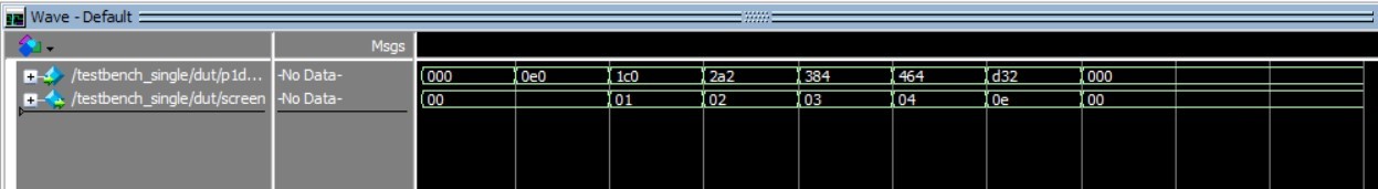
Testing the single player mode began with ensuring that the correct screen state was output. The testbench seen in Figure 6 demonstrates this with 12-bit digital signals between 0 and 3.3 corresponding to their correct screen value.
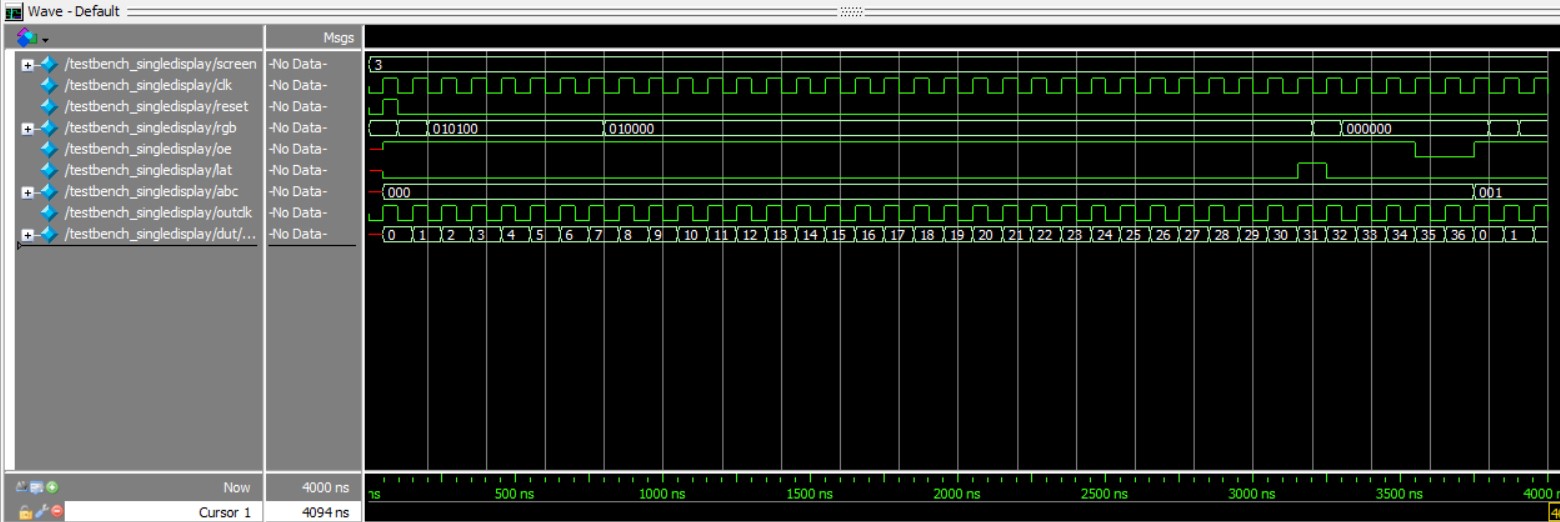
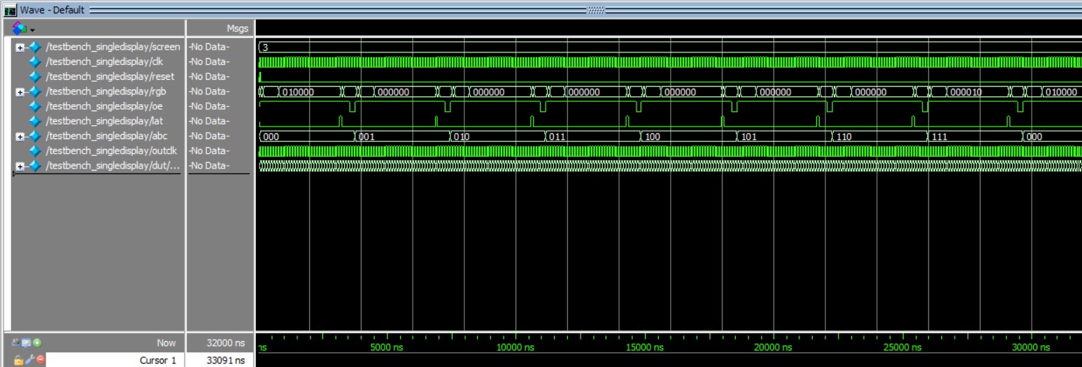
The singledisplay module was a little trickier, but Figure 7 shows the testbench zoomed in to show the clock cycling through the first row state in screen state 3. As seen, rbg for row 0 is consistently 010, so that the upper border is green. Then the rgb for row 8, which is in the middle of the screen is 100 for the first few cycles (state 3 corresponds to a bar that is roughly 4/16 full) and 000 after (when the counter is to the right of the barrier variable). This view also shows output enable being high until the row is switched and lat pulsing once the 32 bits have been written.
Figure 8 shows the testbench, zoomed out to show abc cycling through for a whole screen. For each of the seven abc states, the same process is seen, with rgb values being written for each individual pixel and changes to lat and oe marking the end of the row.
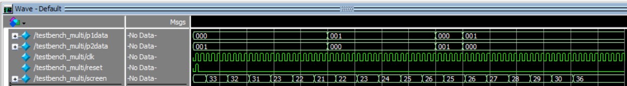
The simulations for multiplayer mode follow a similar process. Figure 9 shows the desired screen being output after reset. Because this mode is sequential, the first four screens are the preset start sequence, and the state changes every 0.715 Hz (a higher frequency is set for the simulation). After the start sequence, the state increases or decreases depending on which player data is a greater magnitude. Once a player reaches the winning state, that state is held until reset.
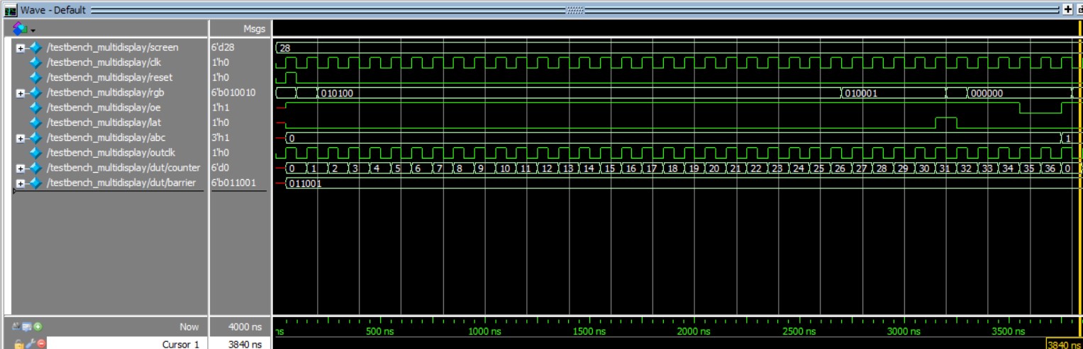
Figure 10 is very similar to the testbench seen in singledisplay but also shows multidisplay at a zoomed in view to show clk cycling through for a whole row.
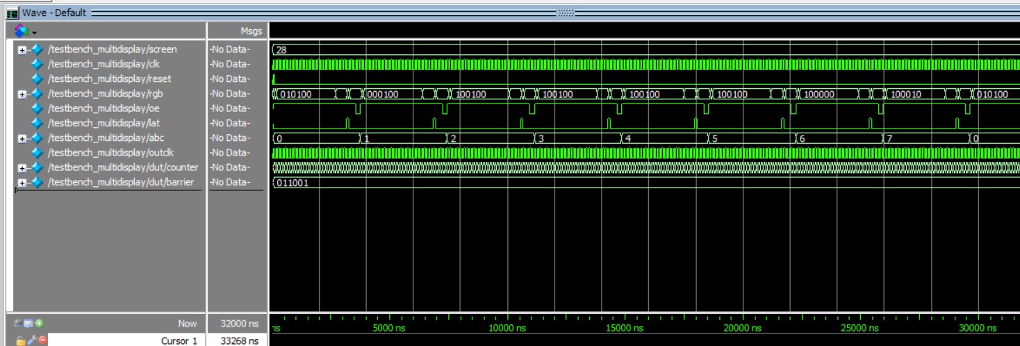
Similarily, Figure 11 shows a testbench of multidisplay zoomed in to show abc cycling through its seven states to light the whole screen.
Discussion
After the SPI module, single and multiplayer processes are run in parallel and then multiplexed before the system output, however this multiplex could also be done earlier to reduce processing power.
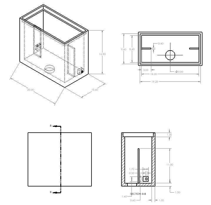
Box
We designed a 3D printed box (Figure 12) to hide and protect all the wires and breadboards. It is a friction fit with the LED matrix on the front. The sensor breadboard goes on the shelf, and the microPs board and breakout go on the bottom. Power enters through the back and sensor wires enter through the sides.